Wide-band dual-pol microstrip antenna on FR4 at 5.7 GHz
By Breadboardhub Staff · Published 2026-08-08
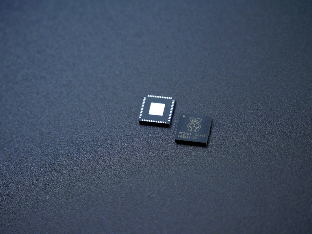
Photo by Vishnu Mohanan on Unsplash
Getting a microstrip patch antenna to be both wide-band and well-isolated between two orthogonal feed ports is genuinely hard, and the usual tricks fight each other. Here is what a recent multilayer FR4 design reveals about how to approach the problem, even if you are working on a more modest bench setup.
Why a plain patch falls short
A standard square patch fed at two edges for dual polarization (one horizontal, one vertical) gives you maybe 2-4% impedance bandwidth on FR4 (relative permittivity around 4.4, loss tangent around 0.02). The two feed ports also couple to each other through the patch, and isolation of 20-25 dB is typical. For Wi-Fi MIMO or any system that needs to reuse the same frequency with two polarizations, you want isolation above 30 dB ideally, and bandwidth wide enough to cover the full 5.725-5.850 GHz ISM band (about 2% of 5.7 GHz, so that part is manageable) or the wider 5.15-5.85 GHz U-NII range (about 12%).
The bandwidth-isolation trade-off is real. Anything you do to broaden bandwidth, like cutting slots or adding parasitic elements, tends to disturb the symmetry the antenna relies on for port isolation.
The multilayer FR4 stackup
The design strategy that makes the numbers work uses a two-copper-layer FR4 board, not a single patch on one layer. Think of it as a standard double-sided PCB where both the top copper and the bottom copper are shaped non-trivially, with the FR4 substrate sandwiched in between.
A typical stackup for 5.7 GHz work:
- Top copper: radiating structure (shaped by optimization, not a simple rectangle)
- FR4 core: 0.8 mm to 1.6 mm thick (thicker helps bandwidth but raises surface waves)
- Bottom copper: ground plane with possible cutouts or shaped features
At 5.7 GHz, a wavelength in free space is about 52 mm. In FR4 it shrinks to roughly 25 mm. A half-wave patch is therefore around 12-13 mm on a side, which fits easily on a standard 2-layer PCB ordered from any fab house.
The two feed ports connect via SMA edge connectors or coax launches on opposite edges of the patch footprint, 90 degrees apart, to excite orthogonal modes.
What topology optimization actually does to the copper
Instead of starting with a rectangle and tweaking it by hand, topology optimization treats every small cell of copper on each layer as a variable that can be solid or void. An algorithm iterates, running a full-wave electromagnetic simulation (typically FDTD or FEM) at each step, adjusting the copper map to simultaneously improve three things:
- Port matching (S11 and S22 below -10 dB across the target band)
- Port isolation (S21 below -40 dB across the band)
- Far-field pattern (stable gain and low cross-polarization in both polarizations)
The result looks nothing like a rectangle. There are irregular copper islands, internal slots, and notches that would be impossible to arrive at by hand. The key insight for a hobbyist is that the asymmetric-looking copper features are doing specific jobs: some slots break coupling paths between ports, while copper stubs on the second layer load the radiating element to shift its resonance and flatten the impedance curve.
You do not need to run topology optimization yourself to benefit from this. The practical lessons transfer:
- Slots cut between the two feed points reduce cross-coupling. Even a simple H-slot or cross-slot between ports can push isolation from 20 dB to 30+ dB on a hand-designed patch.
- A second copper layer with shaped features acts like a broadband matching network built into the substrate, which is more effective than lumped matching at these frequencies.
- Asymmetric copper on the top layer is acceptable as long as the geometry preserves the 90-degree rotational symmetry between the two polarizations. The optimizer finds shapes that look irregular but maintain that underlying symmetry.
Numbers to aim for
The designs in this work achieve around 10% -10 dB impedance bandwidth centered near 5.7 GHz, with isolation better than 40 dB. Measured results matched simulation closely, which tells you the FR4 material model (εr ≈ 4.4, tan δ ≈ 0.02) is accurate enough to design against, provided you order a controlled-impedance stackup from your fab.
For a hand-built version without topology optimization, realistic targets on a 1.6 mm FR4 two-layer board are:
- Bandwidth: 5-8% with parasitic patches or slots
- Isolation: 30-35 dB with a well-placed slot between feeds
- Gain: 6-7 dBi per port
Limitations on a hobbyist bench
Measuring S21 isolation at -40 dB requires a vector network analyzer with good dynamic range and careful port calibration. A NanoVNA can show you whether isolation is in the right ballpark (below -30 dB) but its noise floor and directivity errors make readings below -35 dB unreliable. Solder quality and connector-to-board transitions matter enormously at 5.7 GHz; a bad solder joint adds 0.5 pF that shifts resonance by tens of MHz.
Long jumper wires on a breadboard are completely unsuitable for 5.7 GHz work. This is a PCB project. Even so, a two-layer board ordered from any low-cost fab (JLCPCB, OSHPark, PCBWay) with 1 oz copper and 1.6 mm FR4 is entirely within hobbyist reach, and designing a dual-pol patch with manual slot tuning is a rewarding project once you understand what the optimizer is actually exploiting.
The full design methodology and measured data are described in "Multilayer Dual-polarized Microstrip Antenna Design by Topology Optimization with Enhanced Bandwidth" by Pan Lu, Eddie Wadbro, Viktor Lundström, Jonas Starck, Martin Berggren, and Emadeldeen Hassan, available at arxiv.org/abs/2608.05712.
Attribution
Adapted from “Multilayer Dual-polarized Microstrip Antenna Design by Topology Optimization with Enhanced Bandwidth” by Pan Lu, Eddie Wadbro, Viktor Lundström, Jonas Starck, Martin Berggren, Emadeldeen Hassan, licensed under CC BY 4.0 (https://creativecommons.org/licenses/by/4.0/). Source: https://arxiv.org/abs/2608.05712.
Original arXiv papers: