SpiNNaker2: The Many-Core Chip Bridging Neuromorphic and Deep Learning Worlds
By Breadboardhub Staff · Published 2026-08-02
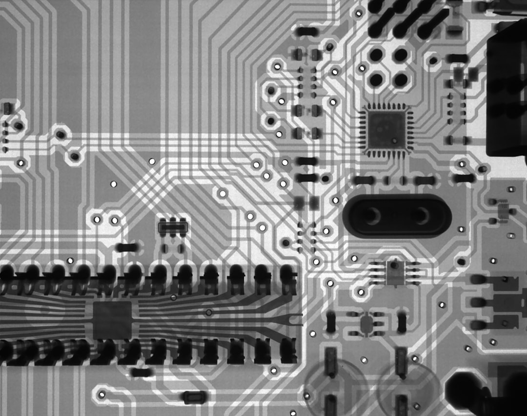
Photo by Mathew Schwartz on Unsplash
A research team spanning Dresden, Manchester, and several European institutions has published details on the SpiNNaker2 chip, a 152-core processor designed to run both conventional deep learning workloads and brain-inspired spiking neural networks (SNNs) on the same piece of silicon. For engineers building edge AI systems, the headline numbers are hard to ignore: 4.5 TOPS peak performance, up to 2.7 TOPS/W efficiency on INT8 inference, and a baseline power draw under 250 mW. That last figure is what separates this from a typical GPU accelerator card and puts it in conversation with the kind of always-on, event-driven systems embedded engineers actually care about.
What Is the Core Finding?
SpiNNaker2 is a single chip that can run deep neural networks and spiking neural networks side by side, without forcing you to choose one paradigm over the other. That flexibility has been the missing piece in neuromorphic research for years.
Most neuromorphic chips available for research, like Intel's Loihi or the original SpiNNaker, were built exclusively around spiking neuron models. They are extraordinarily efficient when your workload matches their architecture, but connecting them into a real product pipeline alongside conventional deep learning inference has always required awkward glue logic and workflow compromises. SpiNNaker2 is explicitly designed to close that gap, letting developers experiment with hybrid approaches that mix standard tensor operations with sparse, event-driven computation on the same device.
How Does the Hardware Actually Work?
Each of the 152 processing elements (PEs) on the chip contains an ARM Cortex-M4F core paired with dedicated hardware accelerators for neural network math. The chip uses an extended version of the original SpiNNaker event-based routing fabric, which is the interconnect that passes spike messages between cores without needing a central bus or clock-synchronized transfers.
For memory and system integration the chip includes an LPDDR4 interface and Gigabit Ethernet, which means it can sit inside a real system rather than just a lab evaluation board. The LPDDR4 interface is particularly relevant for deep learning workloads where weight storage exceeds on-chip SRAM. On the neuromorphic side, the routing fabric can handle more than 1.8 billion synaptic events per second when running SNN simulations at a 1 millisecond time step, supporting networks with over 150,000 neurons. That is large enough to model meaningful cortical circuits or run production-scale SNN inference tasks.
What Does This Mean for Embedded and Edge AI Engineers?
If you are building edge inference hardware today, SpiNNaker2 represents a research preview of where low-power AI accelerators are heading. The sub-250 mW baseline power is genuinely competitive with existing microNPU solutions, and the ability to exploit sparse, event-driven computation means the chip can scale its power consumption down further when inputs are quiet, something conventional dense-matrix accelerators cannot do naturally.
For FPGA engineers who have been implementing custom SNN accelerators in fabric, SpiNNaker2 offers a useful reference point. The event-based routing architecture is a proven design pattern, and seeing it integrated alongside ARM cores and a standard DDR memory interface on a production chip validates many of the architectural choices that have appeared in academic FPGA implementations. The Ethernet interface also hints at the multi-chip scaling story: multiple SpiNNaker2 chips can be networked together, which echoes the kind of scalable inference clusters being built with devices like the Raspberry Pi Compute Module or Nvidia Jetson boards, but with a neuromorphic twist.
What Are the Current Limits?
The paper is a chip-level characterization, not a full software ecosystem release. The 152-core architecture requires careful workload partitioning to extract peak efficiency, and the programming model for hybrid SNN and deep network workloads is still an active research area rather than a plug-and-play SDK.
The 4.5 TOPS figure applies to the high-performance mode for INT8 workloads, and the 2.7 TOPS/W efficiency figure applies to a separate high-efficiency operating mode. You do not get both simultaneously. For comparison, dedicated edge inference chips from companies like Google or Apple can exceed these numbers in pure throughput, so SpiNNaker2's value proposition is specifically in the flexibility to explore event-driven and sparse computation, not raw throughput competition with datacenter-derived accelerators. Developers interested in the platform will need to track the associated software tools and SNN frameworks to understand the practical programming path.
As neuromorphic toolchains mature and hybrid SNN-plus-deep-network models find their first real applications, chips like SpiNNaker2 may redefine what energy-efficient edge inference looks like for the next generation of embedded AI products.
Attribution
Adapted from “The SpiNNaker2 chip: a many-core platform for flexible and scalable brain-inspired computing” by Stefan Scholze, Johannes Partzsch, Sebastian Höppner, Florian Kelber, Andreas Dixius, Marco Stolba, Sirine Arfa, Marc Berthel, Georg Ellguth, Jim Garside, Hector A. Gonzalez, Stephan Hartmann, Thomas Kiel-Hocker, Dongwei Hu, Matthias Jobst, Khaleelulla Khan Nazeer, Tim Langer, Chen Liu, Gengting Liu, Matthias Lohrmann, Mantas Mikaitis, Felix Neumärker, Amirhossein Rostami, Stefan Schiefer, Tilo Schubert, Delong Shang, Bernhard Vogginger, Yexin Yan, Steve Furber, Christian Mayr, licensed under CC BY 4.0 (https://creativecommons.org/licenses/by/4.0/). Source: https://arxiv.org/abs/2607.24396.
Original arXiv papers: